
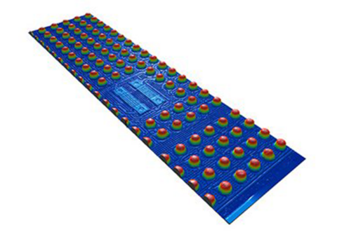
In-Process Wafer Step Height Measurement
Non-contact and non-desctructive optical measuring in the nanonmeter range. During the grinding process the wafer thickness needs to be controlled in real time. A non-contact, optical measurement technology is the ideal solution to monitor the wafer thickness in-process. Optical technology also enables profiling of chip-on-wafer and MEMS during grinding.
Whitepaper Spring 2019
Dies könnte Sie auch Interessieren
计量技术走向半导体创新前沿
这篇Photonics文章重点介绍了先进的计量技术如何走向半导体制造的前沿,从而在先进节点上实现更严格的工艺控制。文章强调了高精度在线测量解决方案(如Precitec 3D Metrology的解决方案)对于确保现代工厂的产量、速度和可靠性的重要性。点击此链接可阅读全文(英文)。

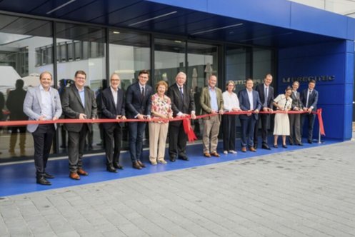
Gaggenau 新大楼落成典礼
普雷茨特发展的重要一步: 几个星期以来,我们已经可以在新的现代化工作场所工作了。这改善了不同部门之间的协作和对话。生产线是一大亮点,它已升级到最新的纯度级别。在一年一度的夏季聚会期间,我们举行了一个小型的落成典礼。
…

Enovasense honored as inVision Top Innovation 2024
Thickness measurement of opaque and semi-transparent coatings with laser photothermal technology.
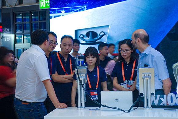
成功举办中国国际信息通信展览会
普雷茨特首次展出高功率智能激光切割头 ProCutter 2.0 60kW,与 CutBox 搭配使用可形成稳定高效的切割组合。焊接产品则提供了以动力电池焊接为主的新能源汽车解决方案。
…

Precitec 印度公司成立
新成立的Precitec印度有限公司的所有未来员工满怀期待地聚集在一起,庆祝新篇章的开始。此次活动充满了热情积极的氛围,展现了员工共创伟业的愿景。
Precitec 管理层负责人 Christof Lehner 对大家的到来表示热烈欢迎,并强调了这一基础对于 Precitec…
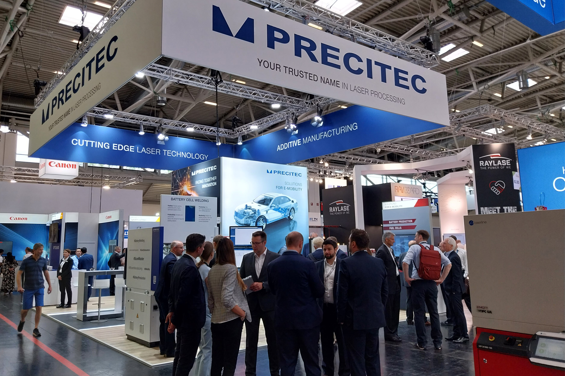
慕尼黑光博会是个杰出的展会。
为期一周的慕尼黑光博会已圆满结束。作为世界领先的激光、光电行业平台,汇聚了大量用户、光源制造商和系统供应商,使得此次盛会尤为重要。
Precitec 很荣幸能够参加这个充满活力的盛会,展示我们在 "电子汽车…
